
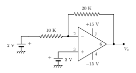
Identify the above op-amp circuit. Estimate the net output voltage V_0.
cse-2010-subject-08-006
Identify the above op-amp circuit. Estimate the net output voltage V_0.
What is Josephson tunnelling? Distinguish between a.c. and d.c. Josephson effects.
Explain the reduced zone scheme of plotting the energy bands in solids. On the basis of E vs k curve distinguish between conductors, semiconductors and insulators.
Distinguish between Einstein and Debye models of specific heats of solids. Obtain an expression for the specific heat of a solid on the basis of Debye model. Discuss the results for low and high temperature ranges.
What do you understand by early effect in bipolar junction transistors ? What are its consequences ? Discuss briefly the advantage of using the BJT in the common collector configuration.
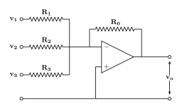
List the characteristics of an ideal OP-AMP. Write the expression for the output voltage in terms of input voltages and resistance values.
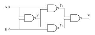
Verify that the circuit shown below is an exclusive OR.
The resistance of silicon and germanium varies with temperature. But these are not used normally as thermistors. Why ? Name at least two widely used materials for making thermistors and give any five applications of thermistor.
Silicon is the most popular semiconductor material used for the fabrication of electronic devices and integrated circuits. Why ? Give at least five reasons.
A type-II superconducting material with superconducting transition temperature T_c is placed in a magnetic field. What is the material state (normal or superconducting or mixed) for (i) T < T_c ; \quad H > H_{c_2} (ii) T > T_c ; \quad H < H_{c_1} (iii) T < T_c ; \quad H_{c_1} < H < H_{c_2} (iv) T < T_c ; \quad H < H_{c_1} (v) T > T_c ; \quad H > H_{c_2} where H_{c_1} and H_{c_2} are the lower and upper critical fields for a type-II superconductor.
Which of the waves out of (i) X-rays, (ii) de-Broglie waves due to electrons or neutrons will be suitable for crystal diffraction ? Justify your answer in terms of energies of these waves for 0 \cdot 1 \text{ nm}.
Show that the reciprocal lattice of a hexagonal lattice is a hexagonal lattice with a rotation of axes.
What is Meissner effect ? Explain the conclusions drawn from the Meissner effect.
A certain colpits oscillator uses a tank circuit with L = 20\text{ mH}; C_1 = 200\text{ pf} and C_2 = 300\text{ pf}. What is the frequency of oscillation ?
How can the NAND-gates be combined to perform the OR-operation ?
Show the volt-ampere characteristics of a solar cell under illumination. Explain the characteristics.
Draw the circuit diagram of a two-stage RC coupled common emitter transistor amplifier. Show how the magnitude and phase of voltage gain vary with frequency. Define bandwidth of this amplifier. An amplifier with open loop voltage gain, A_v = 1000 \pm 100 is available. It is necessary to have an amplifier whose voltage gain varies by no more than \pm 0.1\%. Find the reverse transmission factor \beta of the feedback network used and the gain with feedback.
Explain the switching action of a FET. Two JFETs are connected in parallel with \gamma_{d1} (drain resistance) = 20\text{ k}\Omega, \gamma_{d2} = 30\text{ k}\Omega and g_{m1} (transconductance) = 2\text{ m-mho} and g_{m2} = 4\text{ m-mho}. Find the efffective \gamma_d and g_m.
(i) Transistors are current operated devices, while vacuum tubes are voltage operated." — Explain. (ii) Why are junction transistors called bipolar devices ?
Distinguish between 'soft' and 'hard' super-conductors. Explain how penetration depth varies with magnetic field strength and temperature.