
Show that the NAND gate is a universal gate.
ifos-2014-subject-08-005
Show that the NAND gate is a universal gate.
Explain with the help of a neat diagram the structure of a n-channel FET and its IV characteristics. In what way is an FET different from a BJT ?
A silicon diode operates at a forward bias voltage of 0\cdot 4\text{ V}. Calculate the factor by which the current will be multiplied when the temperature is increased from 25^\circ\text{C} to 150^\circ\text{C} (\eta for \text{Si} = 2).
X-ray of wavelength 1\cdot 4\text{ \AA} is found to be Bragg reflected from (111) plane of an fcc structure. If the lattice parameter of the crystal is 5\text{ \AA}, find the angle at which the X-ray beam is incident on the (111) plane of the crystal.
Prove the following Boolean identity and draw its gates equivalent : Y = \bar{B}(A + C) + C(\bar{A} + B) + AC
In an operational amplifier, the amplifier gain is 10000. The input series resistance is 100\text{ k}\Omega and the feedback resistance is 500\text{ k}\Omega. If the input voltage is 1\text{ volt}, find the exact output voltage and percentage error considering an infinite gain for the amplifier.
What is a thermistor? Discuss static characteristics of a thermistor. What is its time constant?
Write down London second equation for superconductors. Explain how it accounts for the Meissner effect.
Can you comment from the above question whether you can use it to scan surface by microscopy?
For a simple cubic, a face centered cubic and a body centered cubic crystal, determine the atomic packing factor. How many atoms per \text{mm}^2 surface area are there in (100) plane for leads which has f.c.c. structure. The radius of the atoms is 0\cdot 174\text{ nm}.
A power supply using a full-wave rectifier is to provide 100\text{ mA} at 20\text{ V} with no more than 1\% ripple. Calculate the minimum value of smoothing capacitor used. Consider the diode resistance and the resistance of the secondary of the transformer as negligible. Also take ripple frequency as 50\text{ cycles per second}.
(i) What is De Morgan's law ? (ii) Simplify the Boolean expression A + AB + ABC + ABCD
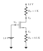
The above circuit exhibits a MOSFET with a source resistor. It has V_T = 1\text{ V} and \mu_n C_{ox} (W/L) = 2\text{ mA/V}^2. Calculate the drain voltage. Also determine whether the transistor is in saturation or in the triode region.
What is Meissner effect ? Determine the magnetic susceptibility of a superconductor. Explain whether a superconductor exhibits perfect ferromagnetism, paramagnetism or diamagnetism.
A type I superconductor with T_c = 7\text{ K} has slope \frac{dB_c}{dT} = -25\text{ mT/K} at transition temperature T_c. Estimate its critical field at 6\text{ K}.
Using band theory of solids, explain whether the effective mass of an electron can be positive, negative as well as infinity. Explain the significance of negative mass.
Explain the basic structure and operation of an n-channel FET. How FET acts as an amplifier ? Explain.
Using OP-AMPs design an analog circuit to solve the following differential equation : \frac{d^2 v}{dt^2} + k_1 \frac{dv}{dt} + k_2 v = v_1(t) with \frac{dv_{(0)}}{dt} = 1\cdot 5\text{ V}; v_{(0)} = 2\cdot 0\text{ V}.
(i) What are intrinsic and extrinsic semiconductors ? Explain. (ii) How are n-type and p-type semiconductors obtained ?
How are the band structures of insulators and semiconductors similar ? How are they different ?