An RC-coupled transistor amplifier has mid-frequency gain A_{\text{vm}} = 100. The values of the lower and upper cut-off frequencies are f_1 = 20\text{ Hz} and f_2 = 50\text{ kHz}. Find the frequencies at which the gain is reduced to 80.
State the Barkhausen criterion for sustained oscillations of a feedback circuit. Explain the operation of a Hartley oscillator using proper circuit diagram.
(ii) Draw a simplified logic circuit for the following Boolean expression : Y = (A + B)\overline{AB}
(ii) Recalculate the intrinsic carrier concentration at T = 450\text{ K} by assuming that the effective electron and hole masses in the respective bands decrease by 0\cdot 5\%.
Consider the planes with indices (1\ 0\ 0) and (0\ 0\ 1); the lattice is f.c.c., and the indices refer to the conventional cubic cell. What are the indices of these planes when referred to the primitive axes : \vec{a}_1 = \frac{a}{2}(\hat{x}+\hat{y}), \vec{a}_2 = \frac{a}{2}(\hat{y}+\hat{z}) and \vec{a}_3 = \frac{a}{2}(\hat{z}+\hat{x})?
Give logic diagram, Boolean equation and truth tables of AND, OR and NOT gates. Show that NAND and NOR gates can be utilized as a Universal Gate.
Given that for intrinsic Si at T = 300\text{ K}, the band gap is 1\cdot 1\text{ eV} and the intrinsic carrier concentration is n_i = 1\cdot 5 \times 10^{10}\text{ cm}^{-3}. (i) Calculate the intrinsic carrier concentration at T = 450\text{ K}. Assume that the band gap at T = 450\text{ K} is 1\cdot 08\text{ eV}.
State the characteristics of an ideal Op-Amp. Explain the use of an Op-Amp as a summing amplifier and a differentiator.
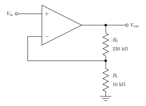
(i) Determine the input and output impedances of the amplifier in given figure. The op-amp datasheet gives Z_{\text{in}} = 2\text{ M}\Omega, Z_{\text{out}} = 75\ \Omega and A_{\text{ol}} = 200,000 (open loop voltage gain). (ii) Find the closed-loop voltage gain.
With a neat circuit diagram, explain the working of Wien-Bridge oscillator.
With the help of a schematic diagram, describe the structure of n-depletion MOSFET. Draw and describe its drain and transfer characteristics.
Consider an n-channel JFET which has \text{I}_{\text{DSS}} = 15\text{ mA} and pinch-off voltage \text{V}_\text{p} = -5\text{ V}. If \text{V}_{\text{GS}} = -1\cdot 5\text{ V}, how much will the drain current \text{I}_\text{D} be? What will be the minimum value of \text{V}_{\text{DS}} for pinch-off to occur at \text{V}_{\text{GS}} = -1\cdot 5\text{ V}?
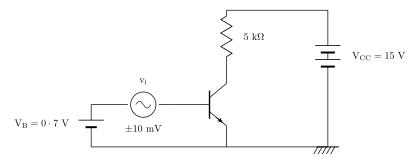
Consider the BJT amplifier circuit given below with the following parameters : d.c. current gain \beta_{\text{dc}} = a.c. current gain \beta_{\text{ac}} = 100 \text{I}_\text{B} = 20\ \mu\text{A} for \text{V}_\text{B} = 0\cdot 7\text{ V}, and \text{i}_\text{b} = \pm 2\ \mu\text{A} for \text{v}_\text{i} = \pm 10\text{ mV}. Determine the values of \text{V}_{\text{CE}}, input impedance and voltage gain \text{A}_\text{v}.
Draw the crystal structure of \text{CaF}_2 indicating the positions of cations and anions. What are their respective coordination numbers?
Derive diffraction conditions using reciprocal lattice concept. What are these conditions known as ?
What will be the frequency of Josephson current, if a d.c. voltage of 4\cdot 0\ \mu\text{V} is applied across a Josephson junction?
Derive an expression for the specific heat of a solid based on the Debye theory and show how it agrees with the experimental values. What is the most important assumption of Debye theory in comparison to Einstein theory ? Is there any drawback of Debye theory ?
(i) Using the logic gates, draw the circuit diagram representing the Boolean expression \text{AB} + \text{A}(\text{B} + \text{C}) + \text{B}(\text{B} + \text{C}). (ii) Simplify the following Boolean expression : [\text{AB}(\text{C} + \overline{\text{BD}}) + \overline{\text{AB}}]\ \text{CD}
Explain classical theory of diamagnetism. Show that the susceptibility of diamagnetic substances is directly proportional to the atomic number. Why all the electrons in an atom contribute to diamagnetism ?
Show that the Fermi level shifts upward, closer to the conduction band in an n-type semiconductor and shifts downward, closer to the valence band in a p-type semiconductor.