(i) Using the logic gates, draw the circuit diagram representing the Boolean expression \text{AB} + \text{A}(\text{B} + \text{C}) + \text{B}(\text{B} + \text{C}). (ii) Simplify the following Boolean expression : [\text{AB}(\text{C} + \overline{\text{BD}}) + \overline{\text{AB}}]\ \text{CD}
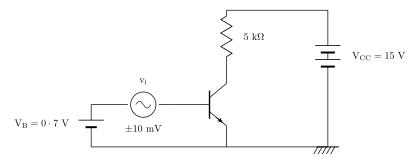
Consider the BJT amplifier circuit given below with the following parameters : d.c. current gain \beta_{\text{dc}} = a.c. current gain \beta_{\text{ac}} = 100 \text{I}_\text{B} = 20\ \mu\text{A} for \text{V}_\text{B} = 0\cdot 7\text{ V}, and \text{i}_\text{b} = \pm 2\ \mu\text{A} for \text{v}_\text{i} = \pm 10\text{ mV}. Determine the values of \text{V}_{\text{CE}}, input impedance and voltage gain \text{A}_\text{v}.
With the help of a schematic diagram, describe the structure of n-depletion MOSFET. Draw and describe its drain and transfer characteristics.
Consider an n-channel JFET which has \text{I}_{\text{DSS}} = 15\text{ mA} and pinch-off voltage \text{V}_\text{p} = -5\text{ V}. If \text{V}_{\text{GS}} = -1\cdot 5\text{ V}, how much will the drain current \text{I}_\text{D} be? What will be the minimum value of \text{V}_{\text{DS}} for pinch-off to occur at \text{V}_{\text{GS}} = -1\cdot 5\text{ V}?
What is Meissner effect? Show that the Maxwell's equation is in contradiction to the Meissner effect. What are the inferences from this contradiction?
State the basic conditions for oscillations in a feedback amplifier. What are the primary requirements to obtain steady oscillations at a fixed frequency?
(i) Diamond and silicon have similar band structure. Why is diamond an insulator while silicon a semiconductor? (ii) An insulator has an optical absorption which occurs for all wavelengths lesser than 1400\text{ \AA}. Find the width of the forbidden energy band for the insulator.
An n-p-n transistor with \alpha = 0\cdot 98 is operated in the CB configuration. If the emitter current is 3\text{ mA} and the reverse saturation current is I_{CO} = 10\text{ }\mu\text{A}, what are the base current and the collector current?
(i) Prove the following using De Morgan's theorems : A \cdot B + C \cdot D = \overline{\overline{A \cdot B} \cdot \overline{C \cdot D}} (ii) Simplify the following expression : Y = A \cdot B \cdot \bar{C} \cdot D + \bar{A} \cdot B \cdot \bar{C} \cdot \bar{D} + B \cdot \bar{C} \cdot D
Describe briefly the functions of the basic segments of a microprocessor. Draw a block diagram of the registers in the 8085 microprocessor.
(i) Distinguish between d.c. Josephson effect and a.c. Josephson effect. Show that Josephson effect exhibits the quantum interference phenomenon on macroscopic scale. (ii) The critical magnetic field of superconducting niobium is 1 \times 10^5\text{ A/m} at 8\text{ K} and 2 \times 10^5\text{ A/m} at 0\text{ K}. Calculate the critical transition temperature (T_c) of niobium.
Explain the high temperature superconductivity. What are different properties of high temperature superconductors ?
Draw the circuit diagram of a transistor operating in the common-base configuration and sketch its input and output characteristics. Indicate the active, cut-off and saturation regions.
When is the channel of a JFET said to be pinched off ? Define the pinch-off voltage. Give the relationship between the pinch-off voltage, the saturation voltage and the gate-source voltage. Sketch the depletion region before and after pinch-off.
Show that the reciprocal lattice for a ‘bcc’ lattice is a ‘fcc’ structure.
When a voltage v_1 = + 40 \mu\text{V} is applied to the non-inverting input terminal and a voltage v_2 = - 40 \mu\text{V} is applied to the inverting input terminal of an Op-Amp, an output voltage v_o = 100\text{ mV} is obtained. But, when v_1 = v_2 = + 40 \mu\text{V} is applied, one obtains v_o = 0\cdot 4\text{ mV}. Calculate the voltage gains for the difference and the common-mode signals, and the common-mode rejection ratio.
Implement the Boolean function X = AB + \bar{A}C using NAND gates.
A transistor operating in the CE mode draws a constant base current \text{I}_{\text{B}} of 30\ \mu\text{A}. The collector current \text{I}_{\text{C}} is found to change from 3\cdot 5\text{ mA} to 3\cdot 7\text{ mA} when the collector-emitter voltage \text{V}_{\text{CE}} changes from 7\cdot 5\text{ V} to 12\cdot 5\text{ V}. Calculate the output resistance and \beta at \text{V}_{\text{CE}} = 12\cdot 5\text{ V}. What is the value of \alpha ?
Describe briefly the construction of an n-channel JFET. Define the pinch-off voltage and pinch-off current. Give the relationship between the pinch-off voltage, the saturation voltage and gate-source voltage.
What is Meissner Effect ? Explain the validity of Meissner Effect in Type I and Type II superconductors.