
Silicon is the most popular semiconductor material used for the fabrication of electronic devices and integrated circuits. Why ? Give at least five reasons.
cse-2009-subject-08-005
Silicon is the most popular semiconductor material used for the fabrication of electronic devices and integrated circuits. Why ? Give at least five reasons.
Explain the switching action of a FET. Two JFETs are connected in parallel with \gamma_{d1} (drain resistance) = 20\text{ k}\Omega, \gamma_{d2} = 30\text{ k}\Omega and g_{m1} (transconductance) = 2\text{ m-mho} and g_{m2} = 4\text{ m-mho}. Find the efffective \gamma_d and g_m.
Draw the circuit diagram of a two-stage RC coupled common emitter transistor amplifier. Show how the magnitude and phase of voltage gain vary with frequency. Define bandwidth of this amplifier. An amplifier with open loop voltage gain, A_v = 1000 \pm 100 is available. It is necessary to have an amplifier whose voltage gain varies by no more than \pm 0.1\%. Find the reverse transmission factor \beta of the feedback network used and the gain with feedback.
Show the volt-ampere characteristics of a solar cell under illumination. Explain the characteristics.
How can the NAND-gates be combined to perform the OR-operation ?
(i) Transistors are current operated devices, while vacuum tubes are voltage operated." — Explain. (ii) Why are junction transistors called bipolar devices ?
Distinguish between 'soft' and 'hard' super-conductors. Explain how penetration depth varies with magnetic field strength and temperature.
Show that FCC-crystals are more closely packed than BCC-crystals,
A certain colpits oscillator uses a tank circuit with L = 20\text{ mH}; C_1 = 200\text{ pf} and C_2 = 300\text{ pf}. What is the frequency of oscillation ?
Simplify the equation: Y = [A \bar{B} (C + BD) + \bar{A} B C] using Boolean algebra. Give the logic circuit for the equation before and after the simplification.
Show that a lattice cannot have a five-fold rotational symmetry. However, some solids appear to exhibit this rotational symmetry. Explain briefly how this can be done.
What is Josephson effect? Discuss briefly DC and AC effects. Give some practical applications of Josephson junctions.
Discuss briefly the concept of effective mass in semiconductors and explain the significance of negative effective mass.
Explain the difference between n-p-n and p-n-p transistors. Give their device structure and biasing circuits. Draw a circuit for a single-stage common-emitter amplifier.
Explain the working of a phase-shift oscillator. Draw the circuit diagram of a phase-shift oscillator using either a transistor or an op-amp. What are the conditions which must be satisfied to achieve stable oscillations ? Calculate the frequency of oscillations for R = 10\ \Omega and C = 0.01\ \mu\text{F}.
Draw the device structure of a p-n junction solar cell and explain how the light energy is converted into electrical energy. Define the 'short-circuit current', open-circuit voltage' and 'efficiency' of a solar cell.
Give the Boolean expression and the truth table for an XOR gate. Why are NAND gates called universal gates ? Realise OR and XOR gates employing only NAND gates.
The following common-emitter amplifier is required to have a signal voltage gain V_{\text{out}} / V_S of at least 100. The transistor has \beta = 63, early voltage V_A = 100\text{ V} and I_{SE} = 1.5 \times 10^{-14}\text{ A} :
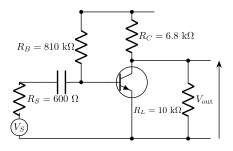
Assuming that the operating collector voltage is supposed to be + 6\text{ V}, perform related calculations to check whether the circuit satisfies the operating point and voltage gain criteria. The reactance of the capacitors can be neglected at all frequencies.
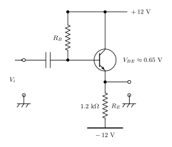
(i) Simplify the logical expression f = ABC + B \overline{C} D + \overline{A} BC by using Karnaugh map and realise f using NAND gates only. 10 (ii) The transistor in the following circuit has \beta = 100 and V_A = 90\text{ V}. What value of R_B will give 0 volt d.c. output 10
Explain the working and applications of a FET.